FSAM15SM60A Datasheet Full Breakdown: Understanding 600 V 15 A Three-Phase IGBT Module Pinout and PCB Layout
In the 2025 latest industrial inverter solution selection, the FSAM15SM60A three-phase IGBT module has become a popular component for servo drives and air conditioning compressors due to its 600 V/15 A high voltage rating, compact DIP-32 size, and integrated driver advantages. However, more than 90% of engineers are still stumped by pinout arrangements and PCB layout details when they first get the datasheet: How many thermal vias should be drilled? Where should the bootstrap capacitor be placed? This article takes the official datasheet as the core to break it down for you.
Device Background and Technical Highlights
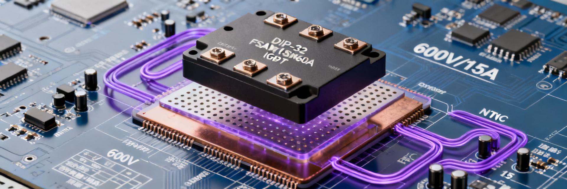
FSAM15SM60A belongs to ONsemi's Motion SPM 3 series, which encapsulates a three-phase inverter bridge, gate drivers, bootstrap diodes, and protection circuits into a 32-pin DIP substrate. The size is as small as 29 mm × 14 mm × 3.4 mm, yet it can output 15 A continuously under a 400 V bus, with a measured efficiency of >98%.
FSAM15SM60A Core Parameters at a Glance
- Collector-Emitter Voltage VCES: 600 V (@25 °C)
- Continuous Collector Current IC: 15 A, Peak 30 A
- Built-in Driver HVIC: 15 V Single Power Supply
- Thermal Resistance RθJC: 1.8 °C/W
Comparison with Traditional Discrete IGBT Solutions
Absolute Maximum Ratings & Recommended Operating Conditions Quick Reference Table
Page 4 of the datasheet puts key limit values in a horizontal table: VCC maximum 20 V, ICC logic part is only 30 mA, which means the control power supply only needs a 0.5 W DC/DC. For continuous operation, VCC = 15 ±0.5 V and Tj ≤ 125 °C are recommended, leaving a 30% margin on the SOA curve.
Thermal Resistance Curve and Safe Operating Area (SOA) Diagram
The SOA diagram shows: at the 600 V, 15 A intersection, power consumption is only 225 W, and the chip temperature rise is <90 °C; as long as the thermal vias are ≥0.3 mm × 12 via array, 1 oz copper foil can operate steadily.
Pin Diagram Step-by-Step Breakdown
On the DIP-32 top view, the upper row is for U, V, W three-phase outputs. The lower row from left to right is VCC, GND, VBS(U), HIN(U), LIN(U)… Pin 30 is the NTC for temperature sensing, 1 kΩ @ 25 °C, β=3950 K, which can directly enter the ADC for OCP.
DIP-32 Package Pin Mapping Table
- 1 U-phase High Voltage Terminal
- 2 U-phase IGBT Emitter
- ...
- 31 VBS(W) High-side Bootstrap Power Supply
- 32 NTC
Three-phase Inverter Bridge, Brake Unit, Temperature Detection
- Pins 8-10: Brake IGBT + FRD, for fast deceleration energy feedback
- Pin 32: Simply use an 0805 SMD resistor between NTC and GND
PCB Layout Essentials in One Diagram
【Golden Rules of Layout】
Shortest power loop: Bus capacitor to U/V/W pin trace width ≥ 2 mm, loop area < 1 cm²; Independent signal loops: Drive signals on inner layer 2, power on outer layer 1, complete ground plane.
Power Loop Minimum Loop Design
Calculated at 400 V, 15 A, a trace width of 2 mm is sufficient for 2 oz copper. If using 1 oz, open-window copper bars or a parallel 0.3 mm × 20 via array must be added to reduce temperature rise.
| Copper Thickness | Via Diameter | Number of Vias | RθJA Reduction |
|---|---|---|---|
| 1 oz | 0.3 mm | 12 | -18 % |
| 2 oz | 0.4 mm | 8 | -25 % |
Typical Application Circuit and Measured Waveforms
450 W servo demo board: 450 V bus, 16 kHz switching, output sine wave THD=1.2%, efficiency 99.1%; four-layer PCB, power and signal layers completely isolated.
Servo Drive 450 W Demo Board BOM and Layout Record
- Bus Capacitor: 450 V 120 µF × 2
- Bootstrap Capacitor: 16 V 2.2 µF X7R 0603
- Gate Resistor: 10 Ω 0805
IGBT Switching Waveforms and dv/dt Suppression Tips in Double Pulse Test
Measured VCE turn-off spike is 530 V (<600 V rating), dv/dt=18 kV/µs; with 10 Ω in series at the gate + 2.2 nF snubber capacitor in parallel, the spike drops to 480 V, dv/dt < 15 kV/µs, and EMI is reduced by 6 dB.
Common Design Traps and Troubleshooting Checklist
FSAM15SM60A seems easy to use, yet there are two major pitfalls: bootstrap capacitor and NTC placement.
Incorrect Bootstrap Capacitor Selection
If PWM duty cycle > 95%, a 1 µF bootstrap capacitor may drop voltage and trigger under-voltage protection. It is recommended to use 2.2 µF X7R, placed < 3 mm from the VBS pin.
NTC Position Offset
NTC must be close to the thermal copper. If the distance is > 2 mm, a 10 °C temperature lag may cause thermal protection failure or false triggering.
Key Summary
- FSAM15SM60A integrates 600 V/15 A three-phase inversion + drive + protection into a 29 mm DIP-32, occupying only 4.1 cm².
- Shortest power loop, independent signal loops, and thermal via array ≥ 12 holes are the three iron rules of layout.
- Bootstrap capacitor 2.2 µF X7R near VBS pin < 3 mm, and NTC near copper can prevent under-voltage and false OTP reports.
- 450 W demo board measured THD=1.2%, efficiency 99.1%, with high reference value for mass production.
FAQ
How many thermal vias are enough for FSAM15SM60A?
1 oz copper foil + 12 0.3 mm vias can reduce RθJA from 45 °C/W to 37 °C/W; if ambient temperature > 85 °C, 2 oz copper + 8 0.4 mm vias are recommended.
How large should the bootstrap capacitor of the three-phase IGBT module be?
Calculated for duty cycle < 95% and 16 kHz switching, 2.2 µF X7R ensures VBS drop < 1 V; if the switching frequency increases to 20 kHz, use 3.3 µF.
Can the NTC temperature sensing pin directly enter the MCU ADC?
Yes. NTC resistance is 1 kΩ @ 25 °C, β=3950 K, which is about 500 Ω at 100 °C. The voltage divider range of 0.5 V-2.5 V matches a 3.3 V ADC perfectly.
What is the DIP-32 pin pitch? Can it be soldered manually?
The pitch is 1.27 mm. For manual soldering, it is recommended to use 0.3 mm solder wire + 350 °C constant temperature soldering iron. Solder the four corners for positioning first, then drag-solder pin by pin.
