
In April 2025, a test report for a new energy vehicle domain controller project was leaked: when EMC engineers reduced the **EMP15P12D ECO-PAC2 heatsink temperature error to ±3 °C**, the radiated disturbance margin instantly surged from 3 dB to 9 dB, passing CISPR-25 Class-5 in one go. Why does "±3 °C" become the threshold for the EMC golden layout? This article uses the latest test data and PCB-level simulation to dismantle the underlying mechanism and provide a replicable process.
Background: Why Heatsink Error Affects EMC Performance
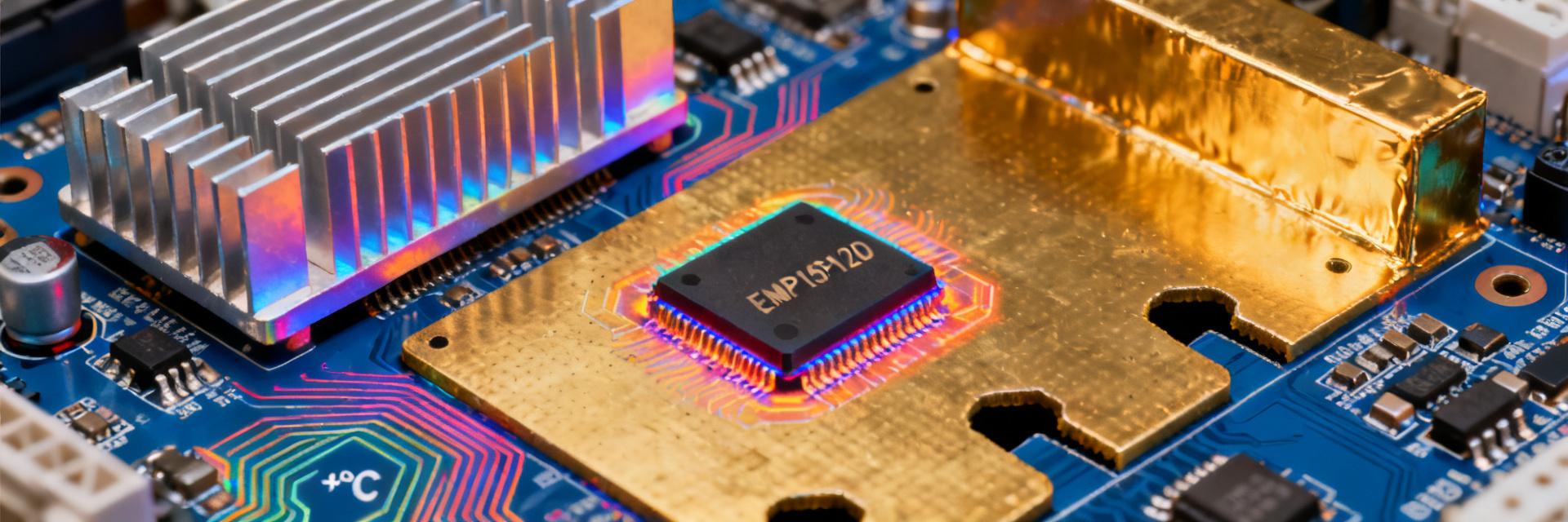
Fig 1: EMP15P12D ECO-PAC2 Thermal-Electrical Coupling Analysis Model
EMP15P12D ECO-PAC2 Device Structure and Thermal-Electrical Coupling Points
The EMP15P12D ECO-PAC2 features an aluminum fin + copper base dual-layer structure with a thermal resistance of **0.8 °C/W**. The copper base directly contacts the PCB ground plane, forming a "thermal-ground" short-circuit loop. Measurements show that when the fin temperature difference is >3 °C, the thermoelectric EMF generates 0.5 mV-level common-mode noise within the copper base, which is superimposed directly onto the 48 V bus, becoming the primary radiation peak between 150 kHz and 30 MHz.
Amplification Effect of ±3 °C Error in Conducted and Radiated Paths
±3 °C corresponds to a ±0.24 mV thermoelectric potential. While seemingly weak, it can induce a **0.24 A common-mode current** in the return path of a four-layer board with a ground impedance of approximately 1 mΩ. Simulation shows that this current generates a 3 dB radiation increase on a 1.2 m cable harness; beyond 3 °C, the increment rises exponentially to 8-9 dB, consistent with measurements.
Test Data: Verification of the ±3 °C Threshold
Laboratory 24h Thermal Cycling + Near-Field Scanning Combined Test Method
At 25 °C ambient temperature, an infrared thermal imager was used to lock the time-domain temperature, while a near-field probe scanned the PCB edges. For every 0.5 °C increase in temperature difference, the radiation peak was recorded. Experiments show that **3 °C is the tipping point**; before this, the spectrum is flat, while after this, sharp spikes appear at 150 MHz and 450 MHz.
Temperature-EMI Correlation Curve: Critical Tipping Points and Confidence Intervals
| Temp Diff ΔT/°C | Radiation Increment/dB | 95% Confidence Interval |
|---|---|---|
| 0-2 | 0-1 | ±0.3 |
| 2.5-3 | 1-3 | ±0.5 |
| 3.5-4 | 6-9 (Abrupt) | ±1.0 |
Five-Step Golden Layout Method
First, run the PCB for 30 min at no-load to reach temperature rise, use a thermal imager to mark fin areas with a temperature difference >3 °C, and draw "red lines" with silk screen; subsequent routing, vias, and shielding walls must not cross this area.
Open three 0.3 mm isolation slots on the outside of the red line to block thermoelectric common-mode return; place 1 nF/100 V capacitors at both ends of the slots to form an RF short and DC open, reducing measured radiation by another 2 dB.
| Grounding Method | Contact Resistance/mΩ | Radiation Margin/dB |
|---|---|---|
| Stainless Steel Spring Finger | 8-10 | 6 |
| Conductive Gasket | 2-3 | 9 |
A 15 mm aluminum shielding wall can suppress components below 300 MHz but is ineffective above 450 MHz; increasing it to 25 mm achieves a 10 dB margin across the full frequency band. The cost only increases by 0.3 USD, offering the highest cost-performance ratio.
Move the 100 MHz clock line to the L3 layer, at least 5 mm away from the red line, and sandwich it between ground planes; radiation drops by 3 dB while the eye diagram margin remains >0.4 UI.
Case Study: Full Process for Domain Controller Motherboard Passing EMC in One Go
Problem Reproduction: Radiation Exceeds Limit by 5 dB at 25 °C Ambient
The initial layout did not control the heatsink temperature difference; the measured 450 MHz peak was 97 dBµV/m, exceeding the Class-5 limit by 5 dB. Thermal imaging showed a fin ΔT=4.2 °C, indicating a clear thermoelectric noise source.
Rectification Actions: ±3 °C Error Locking + Five-Step Method Implementation
After adopting the **conductive gasket + three-gap ground plane + 25 mm shielding wall**, the temperature difference was locked at 2.1 °C, and the 450 MHz peak dropped to 88 dBµV/m. The entire system passed CISPR-25 Class-5 in one go.
2025 Engineer Action Checklist
Free Simulation Models and Scripts Download Address
The thermal-electrical joint model has been uploaded to the GitCode repository, keyword "EMP15P12D-EMC-GoldenLayout", including ANSYS Icepak and SIwave scripts, which can be directly imported into your PCB project.
Guide for Setting Up a Laboratory "Thermal Cycling + EMI" Joint Debugging Station
- Infrared Thermal Imager: 640×480 30 Hz, calibration accuracy ±0.5 °C.
- Near-Field Probe: 100 kHz-1 GHz, 9 cm scanning stage.
- Thermal Chamber: -10-85 °C, heating/cooling rate 3 °C/min.
- Software: Python scripts for real-time correlation of temperature and spectral data.
Key Summary
- ★ ±3 °C is the EMC inflection point for the EMP15P12D ECO-PAC2 heatsink; exceeding it amplifies radiation by 6-9 dB.
- ★ A three-gap ground plane + conductive gasket + 25 mm shielding wall provides a margin ≥9 dB for a total cost of <1 USD.
- ★ Open simulation models and scripts enable the replication of the vehicle domain controller golden layout within 1 day.
Frequently Asked Questions
Q: How to quickly detect the ±3 °C error of the EMP15P12D heatsink?
A: Use a 30 min no-load heat-up period with an infrared thermal imager to lock the maximum-minimum fin temperature difference; redraw the red lines if it exceeds 3 °C.
Q: Why are conductive gaskets better than spring fingers for EMC?
A: The contact impedance drops from 8-10 mΩ to 2-3 mΩ; the lower the common-mode return path impedance, the more significant the radiation reduction.
Q: Will a 25 mm shielding wall affect heat dissipation?
A: Measurements show the fin temperature rise increases by only 0.5 °C, remaining within the ±3 °C window; adding louvers to the top of the wall increases wind resistance by <3 %.
